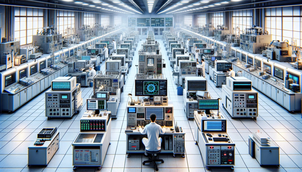
As semiconductor devices become smaller and more complex, advanced technologies are increasingly critical to ensure precision in manufacturing processes. Erik Hosler, a leading expert in semiconductor metrology, underscores the transformative role that artificial intelligence (AI) and machine learning (ML) are playing in optimizing defect detection and improving real-time decision-making in semiconductor inspection. These technologies offer manufacturers new methods to enhance accuracy, reduce downtime, and ultimately improve production yields.
AI-Driven Defect Detection: A Game Changer
Traditionally, semiconductor inspection has relied on human operators and established algorithms to detect defects. However, as the complexity of semiconductor structures increases, the limitations of manual inspection and basic algorithmic approaches become apparent. AI has emerged as a vital tool in overcoming these challenges. By leveraging large datasets and training neural networks to identify patterns, AI-powered systems can detect defects that may go unnoticed by traditional methods.
In the context of semiconductor metrology, AI can analyze massive amounts of inspection data at unprecedented speeds, helping manufacturers identify anomalies faster and more accurately. The self-learning capabilities of AI algorithms allow them to adapt to evolving patterns in semiconductor production, ensuring that defect detection remains effective as new technologies and materials are introduced. This level of automation reduces the risk of human error while freeing up resources for more critical tasks.
Enhancing Real-Time Decision Making with Machine Learning
Machine learning plays a key role in improving real-time decision-making during semiconductor inspection. As devices shrink to the nanometer scale, immediate feedback is essential to ensure quality control and prevent production delays. ML algorithms can process large datasets generated during the inspection process, allowing real-time adjustments to production lines. This not only helps reduce the number of defective products but also optimizes the efficiency of the entire manufacturing process.
By analyzing inspection data in real-time, ML systems can predict potential defects and identify trends that might lead to future production issues. This predictive capability allows semiconductor manufacturers to proactively address problems before they become costly and time-consuming.
AI and ML: Shaping the Future of Semiconductor Manufacturing
AI and machine learning are set to redefine the future of semiconductor metrology. By optimizing defect detection and real-time decision-making, these technologies are enabling manufacturers to push the boundaries of what is possible in semiconductor production. As Erik Hosler mentions, “The ability to detect and measure nanoscale defects with such precision will reshape semiconductor manufacturing.” AI and ML are at the forefront of making this vision a reality, ensuring that the semiconductor industry continues to evolve with ever-increasing precision and efficiency.